-
Latest Version
KiCad 8.0.1 (64-bit) LATEST
-
Review by
-
Operating System
Windows 8 (64-bit) / Windows 10 (64-bit) / Windows 11
-
User Rating
Click to vote -
Author / Product
-
Filename
kicad-8.0.1-x86_64.exe
Schematic Capture
With the schematic editor, you can create your design without limit; there are no paywalls to unlock features. An official library for schematic symbols and a built-in schematic symbol editor help you get started quickly with your designs. Schematic capture is efficient, with all the tools you can expect for such a task. The interface focuses on productivity. There are no complexity limits, as large designs can be divided into hierarchical subsheets. Various export options are available (PDF, SVG, HPGL, Postscript).
PCB Layout
Make professional PCB layouts with up to 32 copper layers. KiCad for PC now has a push and shove router which is capable of routing differential pairs and interactively tuning trace lengths. This modern tool will help you layout your board faster. As you draw your track, it pushes forward traces that are in the way. If that is not possible, your track will be rerouted around obstacles. The push and shove router will make sure that your DRC constraints are respected.
3D Viewer
Ki Cad for Windows 64 bit includes a 3D viewer that you can use to inspect your design in an interactive canvas. You can rotate and pan around to inspect details that are difficult to inspect on a 2D view. Multiple rendering options allow you to modify the aesthetic appearance of the board or to hide and show features for easier inspection. When laying out your PCB, you can instantly inspect your design in an interactive 3D view. Rotate and pan around to inspect details easier than with a 2D display.
Features and Highlights
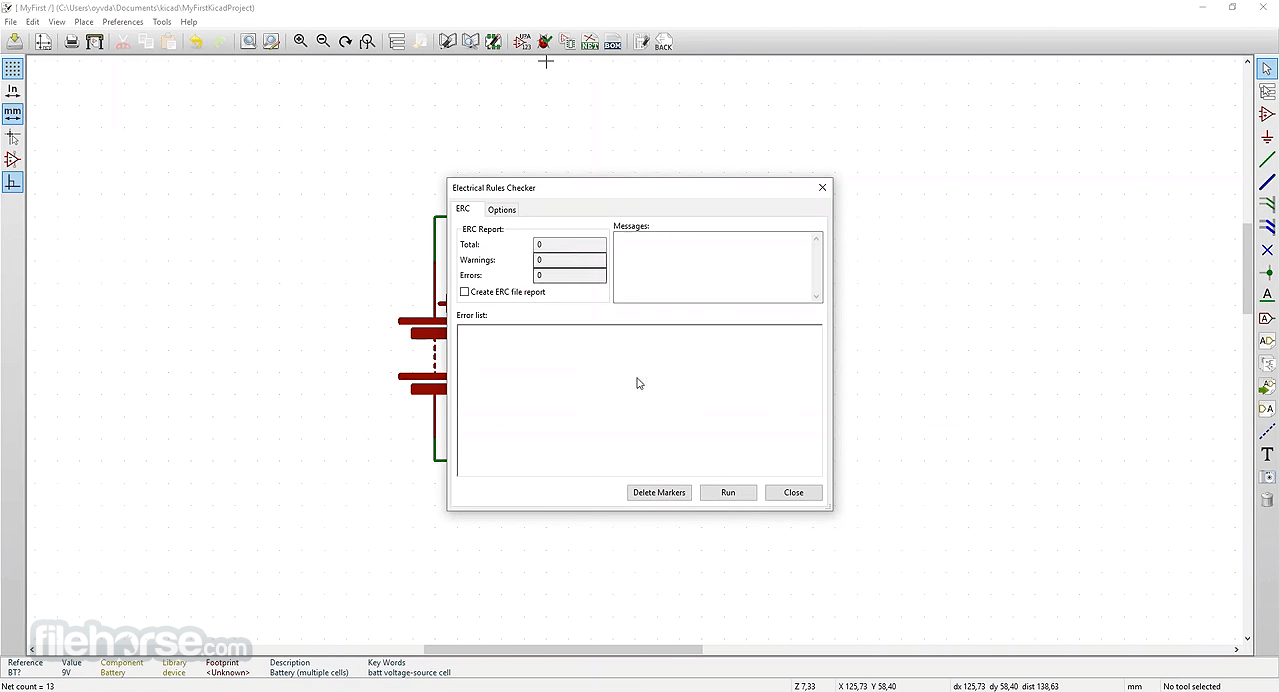
- Electrical Rules Check
- Export Netlists
- Bill Of Materials
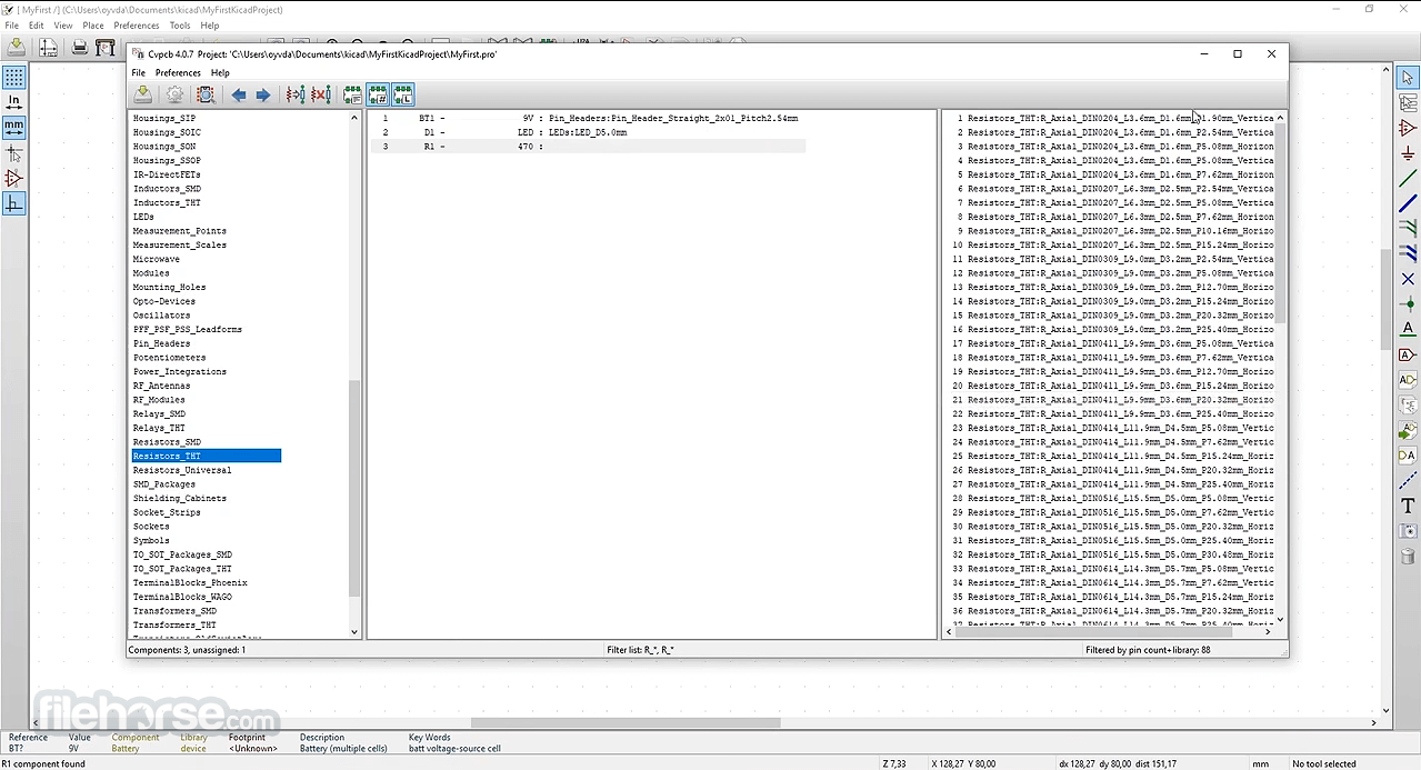
- Integrated libraries
- Push and shove router
- Length tuning
- Footprint Editor (GAL)
-
KiCad 8.0.1 (64-bit) Screenshots
The images below have been resized. Click on them to view the screenshots in full size.

-

-

-
-
What's new in this version:
General:
- Fix custom font rendering issue
- Improve custom font rendering performance
- Update properties panel to use select language
- Make double click open object properties dialog in search panel
- Improve object alignment tooltips
- Use correct text color in library tree selected items on non-OSX platforms
- Fix floating point rounding issues with scaled parameters in settings
- Fix bottom panel background color in footprint and symbol chooser frames
- Don’t import invalid SVG polygons
- Improve fallback (Cairo) canvas performance
- Reduce fallback (Cairo) canvas memory use
- Check environment variable when testing for unresolved variables
- Use a version string without the extra packaging information in drawing sheets
- Don’t show hidden directories and files in the project tree browser
Schematic Editor:
- Fix ghosting when placing multiple label and text objects
- Improve custom rule memberOfFootprint help
- Improve custom rule assertion constraints help
- Do not prevent netclass directive label from being placed when previously placed with no netclass assignment
- Do not reset annotation on reference changes when updating or changing symbols from library
- Improve layout of schematic colors preview
- Set up default netclass wire and bus widths when importing Altium schematic
- Ignore field moves when comparing schematic symbol to library symbol
- Change symbol library search to "and" instead of "or" search terms
- Do not load pin properties as fields when importing Altium
- Select graphical shapes based on effective shape instead of bounding box
- Improve connectivity performance
- Improve responsiveness of some editing operations
- Fix crash when assigning footprint in symbol properties dialog
- Show correct library identifier in change symbols dialog
- Keep schematic text upright when opening V6 schematic
- Fix sheet pin align to grid issue
- Add text size to symbol field properties panel
- Do not draw checkboxes and icons on top of each other in footprint chooser
- Do not overwrite the first item in alternate pin selection list when changing alternate pin
- Fix crash when editing a legacy schematic with missing library symbols
- Prevent silent deletion of entire symbol when using "Edit Symbol Fields" dialog
- Do not print selected item on every page
- Update net navigator when cross probing from board editor net highlight
- Convert legacy schematic descriptions to fields
- Fix crash in zone filler
- Fix crash when ignoring an ERC violation
Spice Simulator:
- Improve tooltips
- Update VDMOS model defaults to ngspice-41 and later
- Fix collecting of signals for S-parameter analysis
- Do not use ohms as units for controlling voltage source parameter
- Handle single source DC analyses correctly
- Only change pin assignments from user interaction
Symbol Editor:
- Update description in library tree immediately when changed in properties dialog
- Improve database library load performance
- Add pin count and footprint filters options to footprint chooser dialog
- Add show/hide invisible pins and fields to view menu and toolbar
- Add KiCad symbol library files to import symbol file selector filters
- Fix crash when switching between two git branches of an open library
Board Editor:
- Properly create bounding hull cutouts for rule area zones
- Do not snap mirrored graphic objects to center of selection when not moved
- Prevent unnecessary move at the beginning of move command
- Prevent duplicate nets when renaming a net in the net inspector
- Rule areas should be allowed on user layers
- Update "Edit Teardrops" dialog to match other teardrop terminology
- Improve teardrop dialog terminology
- Fix teardrop generation when arc track is connected to pad.
- Highlight nets and show length tuning status when adding tuning patterns.
- Add turn off all layers preset option to the appearance manager
- Fix assert and ghost footprint after undoing a footprint drag operation
- Fix broken routing tool immediate mode (X key press) handling
- Fix broken rotated rectangles when importing Eagle boards
- Do not unexpectedly switch focus in board setup grids using the up and down arrow keys
- Improve grid origin action discoverability
- Fix crash when placing vias and using measure tool
- Add option to footprint chooser to switch between the selected footprint or its 3D model
- Fix memory leak in net inspector dialog.
- Fix memory leak when adding tracks
- Reduce undo buffer memory usage when deleting group objects
- Support multi-line text when importing EasyEDA boards
- Fix issue with rounded rectangles in GERBER plots.
- Unflip view when selecting a viewport which isn’t flipped
- Prevent tool re-entrancy when placing vias and using measure tool
- Do not block DRC when schematic parity is check is performed
- Do not extend lines beyond the usable canvas
- Fix crash loading board with undefined net item information
- Rework on bottom panel of footprint chooser to properly display long strings
- Correctly handle circular board outline cut outs in STEP exports
- Correctly handle footprint graphic knockouts for no-net case
- Save and restore corner radius ratio when plotting pads
- Don’t select reference images when they are hidden
- Revert changed rotation behavior for all objects except text boxes
- Fix selection freeze when selecting two zones on the same layer with different nets
- Do not clip output when plotting to PDF
Footprint Editor:
- Improve missing feature warnings when importing Altium footprint libraries
- Draw graphical shapes with correct fill color
3D Viewer:
- Add option to use PCB Editor physical stackup settings as defaults
- Update color changes made in appearance panel
Gerber Viewer:
- Fix broken XOR mode behavior
Worksheet Editor:
- Hide text item properties built in keywords drop down list when changing control focus
- Fix properties frame focus issue.
Python scripting:
- Fix broken Python path on Debian based platforms
Command Line Interface:
- Allow upgrade of legacy and non-KiCad symbol libraries
Windows:
- Fix footprint chooser graphical glitch after task switch
- Fix unselectable footprints in footprint chooser
- Fix crash on pre-1903 Chinese Windows 10 systems when importing EasyEDA projects
 OperaOpera 109.0 Build 5097.45 (64-bit)
 iTop VPNiTop VPN 5.4.0 - Fast, Safe & Secure
 PhotoshopAdobe Photoshop CC 2024 25.6 (64-bit)
 iAnyGoTenorshare iAnyGo 4.0.15
 Opera GXOpera GX 108.0.5067.43 (64-bit)
 Adobe AcrobatAdobe Acrobat Pro 2024.002.20687
 BlueStacksBlueStacks - Play on PC 5.21.150
 Hero WarsHero Wars - Online Action Game
 Data Recovery4DDiG Windows Data Recovery 9.8.6
 TradingViewTradingView - Trusted by 50 Million Traders
Comments and User Reviews